2 Inductor fabrication and PCB assambly
2.1 Inductor Design and Characterization
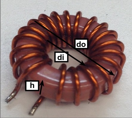
In this lab, you will fabricate your own air-core inductors. You will use magnet wire to manually wind either toroidal air-core inductors (Figure 2.1 (a)) and/or solenoidal inductors (Figure 2.1 (b)).
After fabrication, you will measure their impedance over frequency and extract the parasitic component values of the equivalent circuit model shown in Figure 2.1 (c). Incorporating these parasitics into your simulation will improve agreement between simulated and experimental results.
Therefore, aim to fabricate inductors whose nominal inductance values closely match those used in your simulation.

2.1.1 Toroidal inductor design
The inductance of a toroidal air-core inductor such as the one shown in Figure 2.1 (a) is given by
\[L=\underbrace{\frac{N^2h\mu_{0}}{2\pi}\ln\left(\frac{d_o}{d_i}\right)}_{\text{toroidal component}}{+\underbrace{\frac{d_i+d_o}{4}\mu_0\left[\ln\left(8\frac{d_o+d_i}{d_o-d_i}\right)-2\right]}_{\text{single-turn loop component}}} \tag{2.1}\]
where:
- \(N=\) number of turns
- \(d_o=\) outer diameter
- \(d_i=\) inner diameter
- \(h=\) height
- \(\mu_0=\) permeability of free space
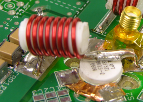
2.1.2 Solenoidal inductor design
For solenoidal air core inductor (see Figure 2.2), you may use the equation attributed to Harold A. Wheeler:
\[L=\frac{a^{2}N^{2}}{9a+10b} \tag{2.2}\]
where:
- \(L=\) inductance in \(\mu\)H
- \(a=\) coil radius (inches)
- \(b=\) coil length (inches)
- \(N=\) number of turns

Equation 2.1 and Equation 2.2 assume ideal winding geometry and are more accurate when the number of turns is large. For this lab, treat these equations as approximate design tools to determine initial coil dimensions.
You may use a plastic form, rod, or a 3D-printed former for winding your inductors. Achieving the exact target inductance will likely require iterative measurement and adjustment of the winding count and geometry.
2.1.3 Inductor Measurement
Measure the impedance of your inductors over a frequency range spanning one decade below and one decade above the switching frequency. Since \(f_s=6.78~\textrm{MHz}\), an appropiate measurement range is \[1~\textrm{kHz}\leq f\leq100~\mathrm{MHz}\]
The impedance Bode plot should resemble the response of the equivalent model in Figure 2.1 (c). Use your measured magnitude and phase data to extract the parameters of the equivalent circuit model that best fit the experimental impedance.
You will use the NanoVNA to perform these measurements. Be sure to calibrate the NanoVNA before taking measurements.
Complete the following tasks:
2.2 Nonlinear \(C_{oss}\) of Si MOSFET
In this lab, you will use the BSC065N06LS5 Si MOFSET from Infineon Technologies. The datasheet and links to the BSC065N06LS5 Si device, as well as links to the device spice models can be found here.
The MOSFET exhibits a nonlinear drain–source capacitance (\(C_{oss}\)) that varies with the applied drain–source voltage \(v_{ds}\). The capacitance variation is shown in Figure 2.3 (Plot #11 in the datasheet).
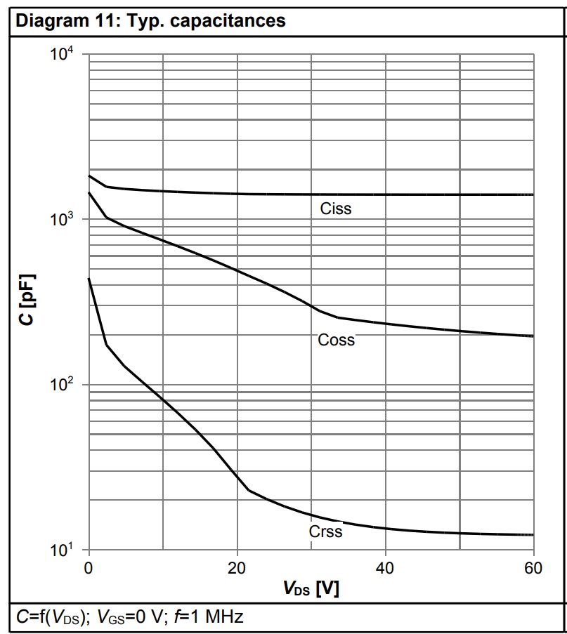
A common approach to account for this nonlinearity in hand design is to approximate the device with a constant capacitance equal to the nonlinear capacitance evaluated at the average drain voltage: %\(C_{oss}(v_{ds})|_{\left<V_{DS}\right>}\)$
Note that Figure 2.3 shows significant variation in \(C_{oss}\) near your operating voltage. Therefore, extracting an accurate value directly from the graph may be challenging. Use simulation-based tuning to refine your design.
2.3 Improved LTspice simulation
Update your simulation as follows:
-
- The manufacturer’s MOSFET model
- The complete equivalent inductor models extracted from your impedance measurements (Section 2.1).
The manufacturer’s model captures the nonlinear capacitance behavior with reasonable accuracy. You may need to retune component values to achieve zero-voltage switching (ZVS), nominal output power, and maximum efficiency (Sokal and Amplifiers 2001). - [ ] Plot three full steady-state cycles of \(v_g(t)\), \(v_{ds}(t)\), and \(v_{load}(t)\). - [ ] Report: - Simulated output power (updated simulation) - \(\frac{\max(v_{ds}(t))}{V_i}\) - Drain efficiency - Maximum voltage across \(C_s\) - Power delivered to the MOSFET gate - Overall power amplifier efficiency - [ ] Update your component value table to reflect any tuning adjustments.
2.4 Power Amplifier stage build-up
As in previous labs, the PCB was designed using KiCad. The GitLab repository containing the design files and annotated schematic is available here.
2.4.1 Interactive BOM
You can use the interactive BOM to assist you when placing the components. Click on settings (the gear icon) and click on full screen.
2.4.2 Assembly Procedure
-
- The Class-E network
- The matching network
- The input decoupling network that will ensure the input voltage remains steady and with low ripple
- Do not solder the MOSFET yet.
-
- The measured impedance
- The simulated impedance (using an LTspice .AC analysis of the passive network only)
Use this comparison to identify discrepancies and adjust component values if necessary. After updating the simulation to reflect the actual board values, include the switch and gate driver models and verify ZVS operation in transient simulation.
2.5 Gate Drive Testing
In this lab, you will use the LM5114 gate driver from Texas Instruments. You can download the datasheet of the gate drive here.
A laboratory waveform generator will provide the input signal via SMA connector (J4).
2.5.1 Pre-Power Checks
After soldering:
- Inspect for solder bridges and loose solder balls.
- Clean the board with isopropyl alcohol (IPA).
- Wear gloves when performing surface-mount soldering.
2.5.2 Initial Gate Drive Test
Once the gate-board is assembled, test the gate drive by doing the following:
-
- \(f=6.78~\textrm{MHz}\)
- \(0~\textrm{V}\) to \(5~\textrm{V}\) square wave
- 50% duty cycle
After confirming proper operation:
- [ ]Install the Si MOSFET.
We need to be careful when doing these measurements by avoiding inserting a significant parasitic inductance. Sometimes, the ground lead of the oscilloscope probe inserts a lot of inductance that affects the measurement. We can improve your high frequency measurements by minimizing the length of the ground lead of the probe. This can be achieved by using a socket for your probe. This video shows a simple way to make a good oscilloscope probe socket.
2.6 Power Board Initial Check
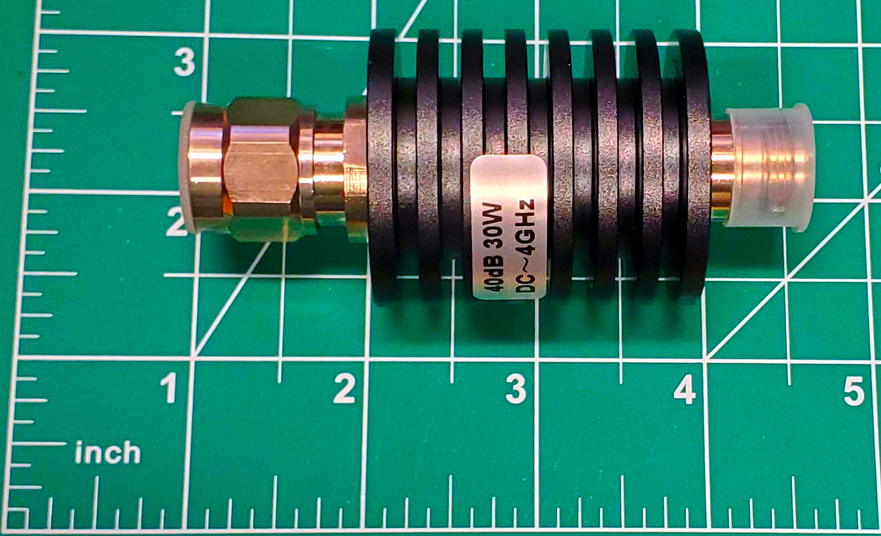
Figure 2.5 shows the simplified experimental setup. The load will be an RF attenuator.

A 40 dB attenuator (Figure 2.6) terminated in \(50~\Omega\) presents a \(50~\Omega\) input impedance. Configure one oscilloscope channel to \(50~\Omega\) input impedance and use a \(50~\Omega\) coaxial cable. The measured signal will be attenuated by 40 dB.
2.6.1 Initial Power-Up Procedure
Once the board is completely assembled, do the following.
Gradually increasing the input voltage reduces the risk of excessive dissipation during tuning. Additional tuning may be required to achieve ZVS and match simulated waveforms. At lower input voltages, the nonlinear \(C_{oss}\) may be large enough to prevent ZVS. As the input voltage increases, the drain–source waveform should approach proper ZVS operation.